Continuous improvements in quality and reduction in early life failures are key goals for semiconductor manufacturers and their customers. Applications most sensitive include vehicle electrification, server, military and defense and consumer goods.
Historically, semiconductor companies would deploy early life failure reduction efforts with electrical tests or geospatial techniques to reject or test out potential failures. Burn-in and predictive test techniques like part average testing have been around for a long time. Additionally, other geospatial methods such as visual defect screening and algorithmic yield clustering looking for abnormal patterns are used to predict early life failures.
Importance of thermal testing in semiconductor design
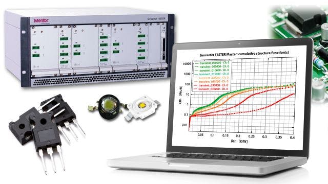
In today’s quest for zero defects and better sustainability, companies must reduce manufacturing errors and variability. Inline thermal resistance measurements add another road to quality for semiconductor companies. Thermal transient testing can measure semiconductor junction temperature responses to short pulses and provide insights to potential manufacturing defects. The technology can reveal inconsistencies in the heat conduction path, quantify their effect on thermal resistance and highlight their location. Problems such as thermal interface material (TIM1) or die attach voids or delamination can be found in a fraction of seconds, but problems outside of the package, such as TIM2 quality can also be measured with short pulses.
Watch this webinar to learn how to use thermal transient testing to measure temperature changes in semiconductor packaging and identify potential manufacturing defects.
Learn advanced thermal testing and die attach techniques in this webinar
Key takeaways from this webinar:
- The role of thermal transient testing to support package model analysis
- Application of structure functions for defect identification
- Testing use cases and limits for package thermal quality
- Different ways of integrating a test system into a semiconductor production environment
Meet the speaker

Andras Vass-Varnai
Portfolio Development Executive for Electronics and Semiconductor
Andras Vass-Varnai obtained his MSc and PhD degrees in electrical engineering at the Budapest University of Technology and Economics. He started his professional career at the MicReD group of Mentor Graphics as an application engineer in 2007. Andras worked most for over 10 years as a product manager, supporting development projects, such as the DynTIM or the Powertester instruments. Before starting his current role as a portfolio development executive for the electronics and semiconductor market in Siemens, Andras worked out of Seoul, Korea, supporting the Asian business activities. He is working out of Chicago, IL currently, with dedicated focus on the US business growth. His main topics of interest include thermal management of electric systems, advanced applications of thermal transient testing and modeling, characterization of TIM materials and reliability testing of high-power semiconductor devices.
