Achieving More than Moore with Heterogeneous Integration
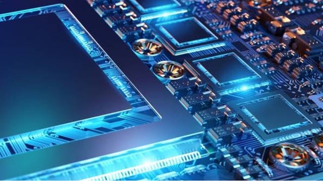
Monolithic System-on-Chip (SoC) design and verification costs are often cost-prohibitive but still need to
achieve More than Moore silicon scaling while managing cost and risk. Alternatives to
monolithic solutions such as SoC disaggregation into chiplets lead to heterogeneous
integration into high-performance package assemblies.
Packaging teams must develop tools and workflows that integrate much tighter ASIC
design processes to achieve advanced heterogeneous designs. Additionally, a new
design flow is required to support the design, validation and integration of interposer
technologies used to interconnect the internal die/chiplets within the 2.5D or 3D
package.
3D IC packaging: heterogeneous integration and hyper-scalability
In this short 15-minute webinar, you’ll learn about heterogeneous integration of chiplets using 3D IC. The primary benefits of this alternative to traditional monolithic SoCs include:
- Reduced area of processor core
- Higher speed processor memory interface
- Increased performance
- Product configurability & scalability
See how your packing design workflows can benefit from the emerging chiplet ecosystem. And, if you’re considering developing or using artificial intelligence, learn why you should consider heterogeneous integration to optimize your designs through specific project objectives.