PCB layout best practices for improved testability and manufacturing efficiency
High-volume printed circuit board (PCB) design has low defect rates. However, batch sizes are falling, and production faults are rising as the sector embraces customization. Most electronics undergo functional testing to ensure proper operation, but when these tests fail, PCB defects are often untraceable, which leads to expensive late-stage rework, delayed product introduction, material waste and defunct boards.
In this webinar, PCB designers will learn the difference between in-circuit tests (ICT) and flying probe tests (FPT) and how best to incorporate automation with either test strategy for early design testability in the layout process.
Maximizing PCB Testability: Automating Analysis for Quality & Efficiency
The means by which a PCB assembly / test process is handled has dramatic effects on product cost, reliability, and time-to-market. ICT and FPT alone are inadequate systems for early testing purposes in PCB production. To achieve better results, PCB manufacturing facilities can efficiently meet their product's cost and quality objectives with specialized equipment that automates each process step, including test strategy.
In this webinar, your PCB design team will better:
- Understand in-circuit and flying probe test manufacturing requirements for electronic PCB design
- Discover how early testability requirements improve production quality
- Explore proper testability guidelines for PCB layout design
- Learn how to choose between flying probe testing and in-circuit testing
- Understand how process test approaches complement functional test needs to produce high-quality products at the right price
Optimizing PCB Test Strategy: How to Incorporate Testability into Layout Design
The goal of the PCB manufacturer involves creating a consistent product at the lowest possible cost with an acceptable fault rate. Therefore, to catch manufacturing errors and component failures early, integrating testability into the layout and design process from beginning to end is critical.
PCB Layout is concerned with the physical design of a printed circuit board and requires initial floor planning, component placement and routing, as well as a consideration of the various types of design. Initial setup will be produced and imported by an outside software like CAD and BOM for accurate test program generation.
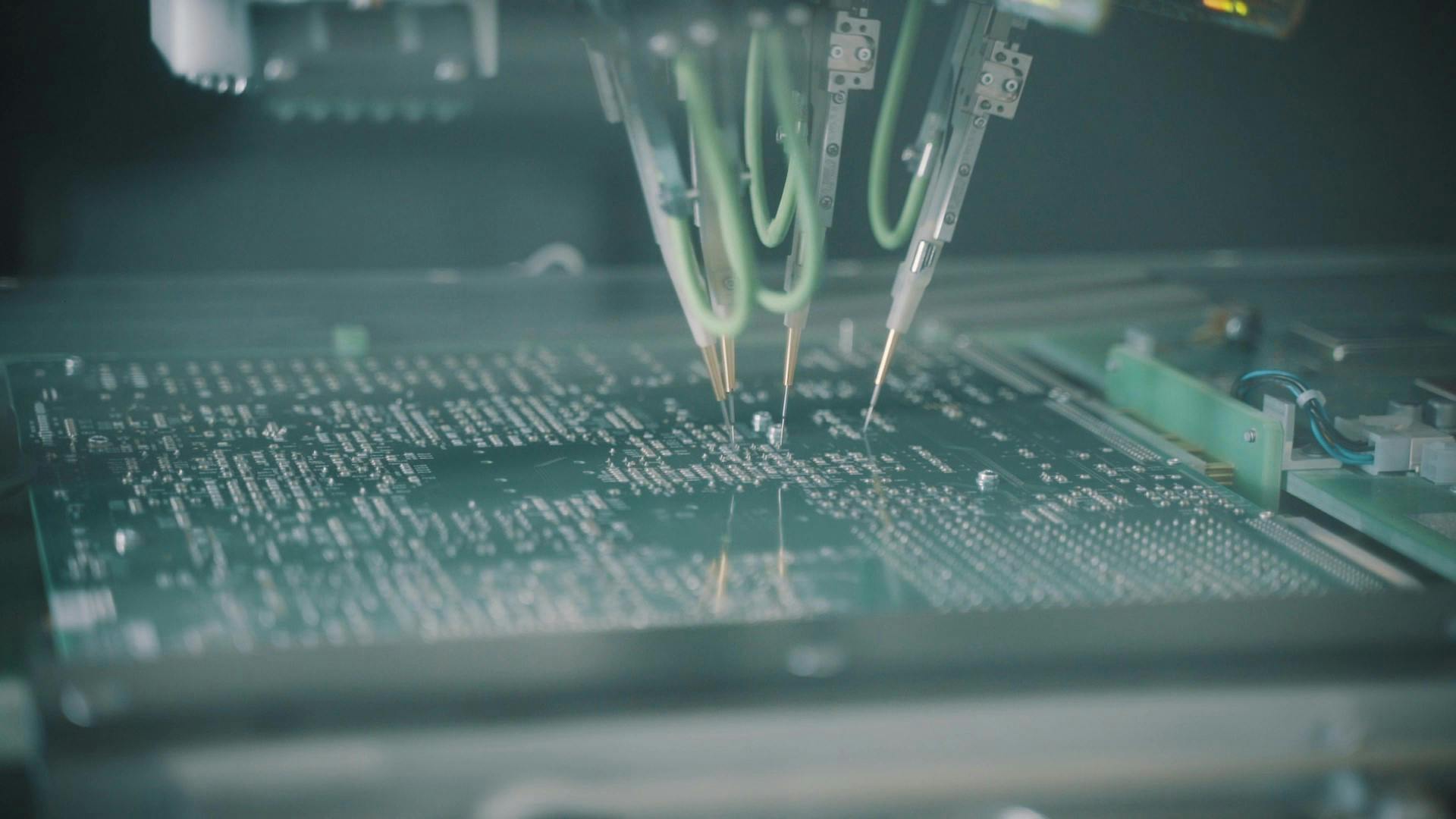
Then depending on which test strategy is chosen, in-circuit testing will utilize a bed of nails interface to connect the test bed to the circuit board or flying probe tests will take individual measurements using robotic arms that move around the board. Each test strategy offers pros and cons that should be taken into consideration to hit specific PCB design targets.
Effective PCB Layout for High-Quality Manufacturing: Automation & Test Strategy
Selecting the best test strategy from the two available options, flying probe testing (FPT) and in-circuit testing (ICT), is essential for effective PCB testing and achieving the best PCB layout.
Once you comprehend the variables at play and understand your product's objectives, the testing strategy will practically choose itself. Questions about your product to ask include high or low volume, long-term requirement or short-term need, quick program turn-around, fast test time, device programming, in-line testing or separate test cell.
Watch this on-demand webinar to learn more about ICT and FPT, and how if the correct test strategy is chosen, the result will be fewer defects, saving the company both time and money, in your PCB design and production.