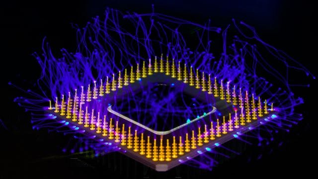
With the rise of 5G communications, Internet of Things (IoT), the development of autonomous vehicles, and edge computing, there is a demand for greater computational power from microprocessors. Consequently, there is pressure on the semiconductor industry to design ever more powerful semiconductor devices with greater functionality yet smaller footprints and lower price points. The result is today's advanced packaging designs using heterogeneous multi-chiplet, 2.5D and 3D integrated circuits (ICs). Semiconductor companies are looking for new system-level design approaches to enhance design productivity and effectiveness.
Watch this webinar to learn about a systemized solution that enables organizations to collate design inputs from architectural fit studies, electrical layout and mechanical models for simulations.
Get the full benefits of digital transformation with model-based systems engineering for semiconductor design
A fully integrated solution allows organizations to get the full benefits of digital transformation through a unified toolchain ecosystem. With end-to-end integration, the integrated high-density advanced packaging workflow includes electrical design, mechanical design, analysis, optimization, and testing and calibration. The integrated workflow reduces iterations and enables earlier thermal or mechanical simulations.
Enhance semiconductor package design productivity and effectiveness with model-based systems engineering (MBSE)
Model-based systems engineering (MBSE) simulations can validate different design parameters, explore alternative designs and determine the optimal solution. Integrating test results plays a vital role in improving simulation model accuracy.
Watch this webinar to learn about:
- High-Density Advanced Packaging (HDAP) market drivers and technical challenges
- A comprehensive end-to-end package design and analysis workflow
- ECAD-MCAD data exchange methodologies, creating package models and package layout implementation
- The addition of detailed package models to PCB designs
- Performing thermal and structural analysis, test-based thermal model calibration
- Design space optimization – driving the design with AI automation
- Integration of test results to enhance model-based systems engineering
Meet the speaker

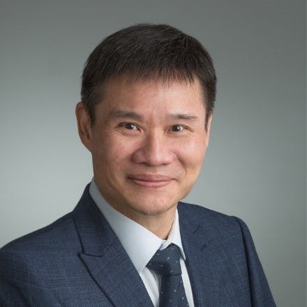
Dr. Hon Wong
Business Development Manager, E&S – Fluid and Thermal
Hon Wong is the Business Development Manager for the Electronics and Semiconductor Industry in the Fluid and Thermal domain for Siemens Digital Industries Software. He is based in Singapore and is focused in the area of semiconductor devices and packaging and works with software and hardware product management teams as well as sales teams globally to meet customers’ requirements.
Hon has over two decades of experience of using thermal simulation tools such as Simcenter Flotherm, Simcenter Flovent and Simcenter FLOEFD for a myriad of flow and thermal related problems. He is also experienced in the Energy, Building and Process industries, etc. using CFD solutions. He was previously with BHR Group, Flomerics, Vestas and Mentor Graphics. He received his Bachelor of Engineering degree from the University of London and holds a PhD. from Cranfield University.
