Implementing design for test (DFT) in 2.5/3D designs using Tessent Multi-die software
Tessent Multi-die software automates complicated 2.5D and 3D IC design for test (DFT) operations
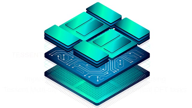
The 2.5D and 3D designs of next-generation IC devices are becoming more sophisticated. Dies that are positioned vertically (3D IC) or side-by-side (2.5D) can pose considerable testing difficulties for ICs.
Siemens Tessent Multi-die software solution streamlines, accelerates and automates crucial design-for-test (DFT) functions for next-generation 2.5D and 3D integrated circuits (ICs).
Implementing Design for Test in 2.5D and 3D IC Designs: What You Should Know
Watch this on-demand webinar to learn how:
- Tessent Multi-die supports the IEEE 1838 standard, including how Tessent Streaming Scan Network (SSN) can be used as the Flexible Parallel Port (FPP) for the standard
- Tessent tools can help with DFT implementation for 2.5D/3D ICs
- Interconnect boundary scan-based patterns between the dies can be extracted using Boundary Scan Description Language (BSDL) from individual dies for 2.5D designs. Plus, unified package level BSDL creation in both 2.5D/3D devices
- IJTAG complements both 2.5D and 3D test
Who would benefit most from watching Implementing Design for Test (DFT) for 2.5D and 3D IC designs?
Anyone who needs to effectuate DFT in 2.5D/3D IC design should learn more about implementation. Professionals in the following roles will find value in this on-demand webinar:
- DFT engineers
- Test engineers
- Senior DFT managers
- CAD directors
Tessent Multi-die: part of the comprehensive Siemens 3D IC design flow solution
The Siemens 3D IC Design Flow is a comprehensive set of tools and workflows targeted to develop advanced 2.5 and 3D IC heterogeneous system-in-package (SiP) designs. This proven, complete 3D IC design flow includes 3D architecture partitioning to planning, layout, design-for-test, thermal management, multi-die verification, interconnect IP, manufacturing signoff, and post-silicon lifecycle monitoring. Transform existing design and IP architectures into chiplets or build scalable 3D IC technology for faster time to market.
Meet the speakers
Vidya Neerkundar
Product Manager - Tessent
Vidya Neerkundar is a Product Manager for the Tessent product family at Siemens Digital Industries Software. She has over 20 years of experience in various DFT aspects with respect to hierarchical flows and architectures including Scan, Test points, boundary scan. Vidya has worked as ASIC design engineer for Conexant prior to joining Siemens EDA. Vidya holds a Master of Science degree in Electrical Engineering.
Joe Reynick
Product Engineering Manager - Tessent
Joe Reynick is a Product Engineering Manager for the Tessent product family at Siemens Digital Industries Software, where his responsibilities include packetized scan and Tessent Multi-die support. Joe has more than 38 years of industrial experience in ASIC Design, DFT, IP, Test and EDA technologies.
Joe served as Director of DFT Solutions at eSilicon, a pioneer of the fabless ASIC and COT models, from 2001 to 2020. His role included building and managing the worldwide DFT team, as well as the silicon bring-up/IP verification labs. His responsibilities included several 2.5D/5.5D projects.
Joe developed his passion for DFT as a member of the technical staff at AT&T/Lucent Bell Laboratories with a focus in the areas of DFT, ASIC Design, Optoelectronics, Test and EDA from 1984 to 2001.