Eliminate PCB Design Spins with automated verification and simulation
Webinar Overview
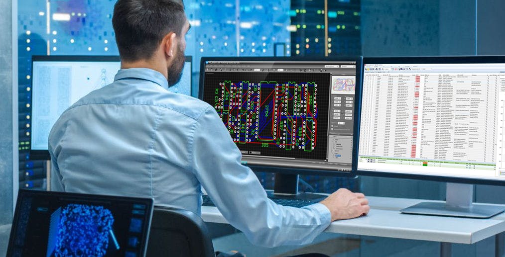
The use of analysis often and throughout the board development process results in reaping tangible benefits by achieving on-time design release without resource surges or higher re-spins. With the ever increase in the design complexity and need for optimizations, there is a need to re-invent the approach towards validation and move the verifications & simulations to early phases of design process. This 'left shift' approach enables Hardware & Layout designers to validate within their native environment, minimizing the bottleneck waiting for specialist reviews and freeing specialists to resolve the remaining critical issues. This webinar walks you through the design challenges and systematic automated and analytical approach used throughout the design process to address these challenges right from schematic validation, Signal and Power Integrity, Electrical sign-off, and Manufacturability.
What You Will Learn:
Who Should Attend
Topics Covered
Meet the speaker

Amit Somanagoudar
Field Application Engineer