Designing a LIDAR application with Siemens/Optiwave using the HHI PDK
This webinar will show how Siemens EDA Silicon Photonics tools increase your design productivity while working with a real-world LIDAR design. Siemens’s Silicon Photonics flow works in conjunction with the HHI PDK and Optiwave optical simulator. Optiwave Systems Inc. is the emerging leader in the development of innovative software tools for the design, simulation, and optimization of components, links, systems and networks for the dynamically growing fields in photonics nanotechnology, optoelectronics, optical networks and other photonic applications.
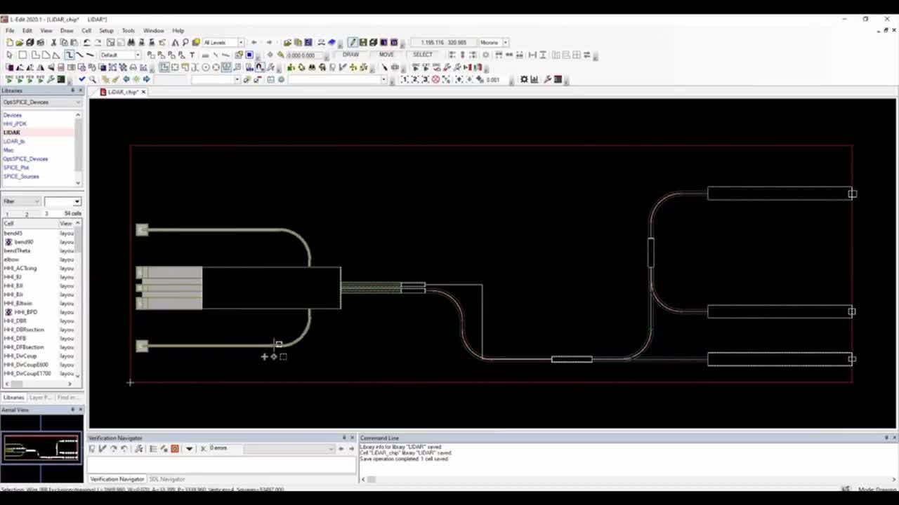
OptiSPICE plugin is a SPICE native optical compact model library designed to integrate into EDA tools. In this webinar, OptiSPICE L-Eit plugin, Siemens EDA and Fraunhofer-HHI PDK is used to design and simulate a LIDAR chip with Homodyne detection. Since 2016, Fraunhofer HHI is offering foundry services for InP based photonic integrated circuits. Designers of this technology can leverage its unique advantages such as optical gain and high E/O efficiency. The PDK contains a variety of lasers, optical amplifiers, modulators and detectors for 56 Gbaud.
What you will learn
Siemens EDA, Optiwave, and HHI will demonstrate a LIDAR design taking
advantage of our tools to increase designer productivity and HHI
foundry services to meet design and time to market needs.